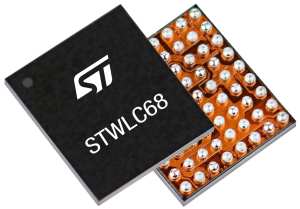
The STWLC68 is our newest wireless power receiver for applications ranging from 5 W to 20 W. Compatible Qi 1.2.4, it offers a proprietary mode that allows customers to implement their fast-charging solution to outpace the competition. The device also distinguishes itself thanks to a unique architecture that pushes the output voltage to a maximum of 20 V, which means that engineers can use an electric current with a lesser intensity to arrive at the 20 W output, thus improving efficiency. Similarly, its digital core manages the main low dropout (LDO) to limit the power dissipation further. It is a crucial point since the STWLC68 will end up in small devices like smartphones, wearables, or medical equipment, among others, and its transmit mode capability means that it can also serve to charge other terminals wirelessly.
The new device replaces the STWLC33, our first 15 W wireless charging solution that we presented in 2017. At the time, wireless charging was starting to make a dent in consumer markets, and the Qi 1.2 Extended Power Profile offered a standard way out of the traditional 5 W systems and into solutions that could manage three times that. It was also one of the first devices to offer reverse charging. Today’s landscape is fascinating because companies are now looking to go beyond the 15 W and provide proprietary solutions that allow their customers to charge their mobile systems even faster and more efficiently, while still offering transmitting capabilities. The STWLC68 thus draws from its predecessor but improves its architecture to satisfy the new reality shaping wireless charging.
STWLC68 and Efficiency, a Smart Core and a More Powerful Voltage Management
 The architecture of the STWLC68 rests on a 32-bit Cortex core, which means that developers can load settings into its One-Time Programmable memory and use it as a standalone chip, or use its I2C interface to adapt its parameters to various use cases. The MCU is also responsible for managing the main LDO linear regulator, which accounts for most of the power dissipation. The use of a digital controller enables a lot more precision, which in turn reduces losses and increases efficiency. We also ship a firmware that takes advantage of sensors within the device to adjust the STWLC68 and minimize losses at different spans along the charging curve, which enables us to offer high power while keeping the temperature low.
Similarly, by offering an output voltage of 20 V, engineers only need to use one ampere to arrive at 20 W. Traditionally, a competing wireless receiver of this size tends to stop at 9 V or 12 V, which means that teams must double the intensity of the electrical current to arrive at the same power output. However, this has the unfortunate consequence of vastly increasing the temperature of the coil and the I2C losses. We were able to jump from the 12 V of the STWLC33 to the 20 V of the STWLC68 thanks to significant improvements in our manufacturing processes. Similarly, these optimizations also enable us to allow engineers to fine-tune the output voltage in steps of 25 mV, whereas the competition can’t handle steps of less than 100 mV. It is particularly crucial for teams looking to optimize a design to increase its efficiency further precisely.
StWLC68 and Prototyping, Starting With the STEVAL-ISB68RX and

The best way to start prototyping with the STWLC68 is to get one of two development boards. The STEVAL-ISB68RX is a classic system that meets the Qi 1.2.4 BPP (5 W) specification. Out of the box, it showcases many of the safety mechanisms of the device, such as its overtemperature, overcurrent, and over-voltage protection, as well as its foreign object detection. Thanks to its USB-to-I2C interface, users can connect the board to a PC, download our STSW-ISB68GUI graphical user interface, and configure the STWLC68, which dramatically facilitates developments. Additionally, the P5 connector allows developers to access some of the device’s GPIO, or connect a temperature sensor.
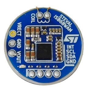
The STEVAL-ISB68WA serves more as a reference design for wearable applications. It limits the maximum power to 2.5 W, but it contains the board and the coil in a design that’s only 15 mm in diameter. Despite its small size, the PCB still offers probing areas to facilitate debugging, and it comes with a USB-to-I2C dongle to also enable the use of our GUI, despite the absence of a physical USB port on the board, due to its size. We provide a user manual that shows how to solder cables that will serve to connect the dongle and how to use our reference design with the STEVAL-ISB045V1, which serves as a transmitter. We thus provide all the tools and documentation to ensure engineers can rapidly build proof-of-concept.
Click Link:
STWLC68: Our First 20 W Wireless Power Receiver With 20 V Output Voltage

No comments:
Post a Comment