- Programme aims to find, facilitate and mentor semiconductor and IP design startups to increase Fabless chip designing in India
- A vital step to strengthen the core Technology-driven System pillar of the Atmanirbhar Bharat and Make in India vision
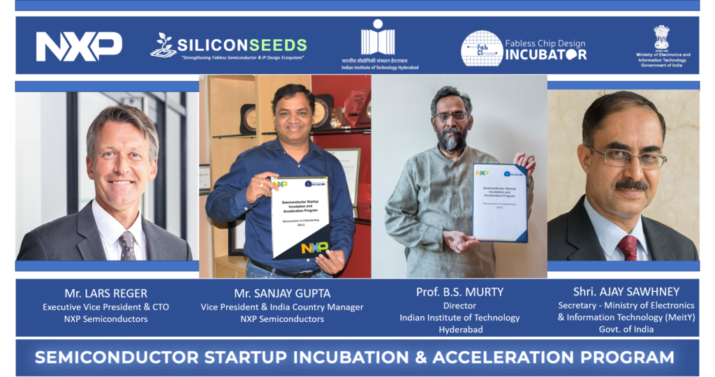
INDIA March 25, 2021: Keeping in line with our Hon’ble PM’s vision of Atmanirbhar Bharat, NXP India, one of the biggest R&D centres for NXP Semiconductors and a world leader in secure connectivity solutions for embedded applications, in collaboration with Ministry of Electronics and Information Technology (MeitY), Government of India and Fabless Chip Design Incubator (FabCI), IIT Hyderabad has announced the launch of its maiden ‘Semiconductor Startup Incubation and Acceleration Program’. The objective of this program is to find, facilitate, and mentor semiconductor and IP design start-ups across India in technological as well as business aspects.

The programme will support India’s vision of making the country a self-reliant nation as it creates a ready platform to support start-ups who wish to design semiconductor chips in India. The local hardware designing and manufacturing of products will strengthen the core Technology-driven System pillar vision of Atmanirbhar Bharat and in turn will boost India’s economy, generate employment, and enhance India’s position globally in the electronics industry by moving up in the value chain.
“The last 10 years in electronics have been all about connecting the world and providing On Demand experiences. Today you can easily order transportation, food or other goods in the “here and now” without moving. The next decade will be all about creating a “world that anticipates & automates” with a lot of smart connected systems around us. All of that will lead into making the planet a better world to live in and fun to innovate in. These smart connected systems have a core semiconductor technology at the heart of it. In that context, I see Semiconductor Startup Incubation and Acceleration program can bring the core impetus to the strengthening of fabless semiconductor design in India and I am very excited and looking forward to see the outcomes with this program” said Lars Reger, Executive Vice President and Chief Technology Officer, NXP Semiconductors.
Expressing his excitement at the launch, Sanjay Gupta, Vice President and India Country Manager said, “At NXP India, the team has consistent focus on building the Indian technology ecosystem for a Win-Win. When our Hon’ble Prime Minister Mr. Narendra Modi gave a clarion call to all the Indians to work towards transforming into next emerging technological & innovation focus country in the world, Team India got into a thinking mode and today I am extremely proud to see their efforts finally taking shape. In this endeavor, Team India has created a technology startups focused framework with two key initiatives – Tech startup challenge to recognize most innovative Indian Startups products aligned to NXP businesses and technologies and Technology Startup Incubator to nurture and groom young startups with complete enablement, funding and day to day guidance using a unique collaboration with Govt. of India and top Academic institutes. We are certain that the enthusiastic and budding entrepreneurs of our country will benefit immensely from this program”.
Sh. Ajay Sawhney, Secretary, Ministry of Electronics and Information Technology (MeitY), Government of India, said, “The Government of India has been working towards promoting the ESDM sector to bring electronic manufacturing to India. There is also a need to build a thriving fabless design ecosystem in India. We look forward to this joint initiative of NXP Semiconductors and IIT Hyderabad for this Incubation cum Accelerator Program that aims to find, facilitate and mentor the semiconductor and IP design startups pan India. It is a significant step as India is poised to increase its share in innovation-driven global manufacturing of mobile phones, IT hardware, automotive, industrial and medical electronics, IoT and other devices.”
Highlighting the uniqueness of the FabCI at IIT Hyderabad, Prof. B.S. Murty, Director, Indian Institute of Technology Hyderabad, said, “This collaborative effort is an much needed, perfectly timed impetus to usher in, an era of semiconductor ecosystem in India. The endeavors carried out by IIT Hyderabad under the aegis of MeitY to set up Fabless chip design Incubator (FabCI) is the building block of this program. FabCI is an unique incubator that provides free access to highly expensive EDA tools and prototyping, apart from the basic infrastructure. With the advent of Atmanirbhar Bharat, more no. of start-ups are expected to come-up across various segment of technology and Incubators like FabCI with support of Technology experts like NXP will definitely strengthen the start-ups ecosystem in the semiconductor industries.”
Unique features of the program:
• Upto Five promising start-ups will be incubated for a period of two years in each cohort every year. The participants will include Semiconductor Chip Design, IP Design, Design Services startups with an IP focus and Chip Design Tool related startups.
• Invaluable experience opportunity for start-ups to showcase their products to investor and business community
• Startup selected for the core program will have the following benefits (with benefits accruing upto INR 1crore per year per startup): EDA Tool Access for design and simulations, Mentoring Access during design and development phase, Selective IP Access for processor or interconnect aspects, Foundry/Packaging Access, Characterization Lab Access, Demo day visibility with NXP.
No comments:
Post a Comment