The latest fixtureless technology available for production and validation testing the most challenging Probe Cards
Strambino, July 2021 — Wafer fabrication is a sequential or “front end” process that starts to create the electronic circuit.
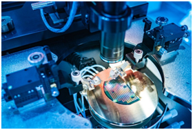
The manufacturing process of silicon wafers simplifies the process and allows many integrated circuits to be placed onto a semiconductor wafer. This wafer is then diced and packaged. Before the dicing is performed, the circuits need to be tested. This electrical test is carried out with the help of a probe card.

What is a Probe Card?
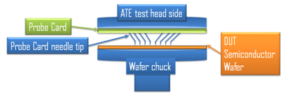
A Probe Card is basically an interface that provides electrical and mechanical contact between the device under test [DUT], which is the semiconductor wafer, and the test system electronics.
A Probe Card consists of the following elements:
• The Multilayer Organic substrate (MLOTM)
• The Printed Circuit Board (PCB)
The wafer test system is composed of different parts:
• The wafer under test [DUT] is presented to the Wafer chuck
• The Probe Card is docked onto the wafer and it serves as a connector between the bonding pads of the DIEs and the test system.

How probe cards are tested?
We have seen that the Probe Card is a critical part of the wafer test system, and it is mandatory to test it before integrating it into the wafer test system. When the device I/O bandwidth and the power demands increase, it is necessary to meet the requirement for high performance power and signal delivery during the electrical test. These requirements drive the challenges for the testing of the probe cards.
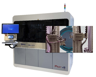
Thanks to many years of experience in testing probe cards, Seica has designed the PilotV8XL HR Next> series, which is the ONLY flying Probe that can offer a full turnkey solution for the Probe Card test.
The PilotV8XL HR Next> series brings together in a unique system three different tools and solutions to perform a complete test, they are:
• Bare Board Test for single MLO & PCB Test
• ICT & Functional Test for assembled PCB Test
• Probe Card Test for PCB+MLO
Along with the three test strategies above the PilotV8XL HR Next> series ensures ICCT (Integrity Connection Certification Testing). This ICCT is a requirement for certification for the integrity of the connections between the MLOTM and PCB.

Pilot V8 XL HR Next> series Hardware Features
The main hardware characteristics of the Pilot V8 XL HR Next> series are:
• Vertical Platform (easy to load and unload all board types including round boards)
• 8 Full independent axes
• Front side: 2 standard probes + 2 HR (high resolution) probes
• Rear side: 4 standard probes
• Large test area: 800 x 650 mm
• Laser sensor(s) for full warpage control
PilotV8 XL HR Next> series “takes care” of MLO pads
pads
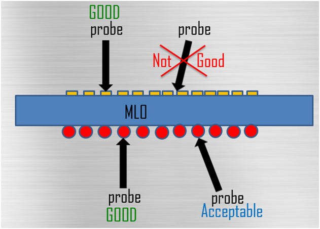
With any sensitive product to test it is mandatory to balance the probe contact force in order to not leave witness or scrub marks on the pads or wafers to be probed.
The best approach to not have any visible mark on the Die pads are to have a Z movement perpendicular to the MLO . With this approach, the prober can guarantee the best touch possible without leaving any witness/scrub marks.
Any other different angle in the movement of the Z axis will increase heavily the chance to leave a scratch on the Die pads.
When the probe card is fully assembled and the MLO is mounted on the PCB interface, the final ICCT test must be performed in order to test the integrity of each single connection between MLO
 and PCB interface itself.
The PilotV8 XL HR Next> series will generate automatically the specific tests taking into account the resistance of each single path that can be different from one to another.

No comments:
Post a Comment