Wondering how professionals inspect Quad-Flat No-leads (QFN) components on the Printed Circuit Board (PCB)? For these components to operate optimally, manufacturers must identify defects and correct them right at the point of production.
In this regard, we shall discuss how to inspect QFN components using the best PCB X-ray machine.
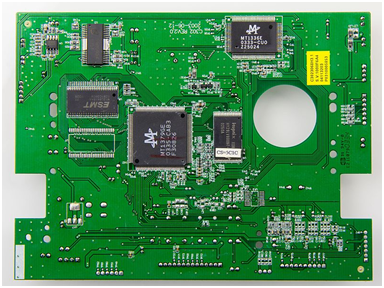
To start with, it’s important to appreciate how technology has improved over the years. With these technological advances, QFNs, where integrated circuits are connected to PCBs, have become popular in almost all electronics.
The need for ‘small’ has led to a noticeable seismic shift toward component miniaturization. As consumers’ demand for more functionalities in smaller packages rises, the need for innovative products such as the Quad Flat No Leads (QFN) packages also rises proportionately.
Why Do You Need To Inspect QFN Components?
While we’re persuaded beyond any reasonable doubt that inspecting a product after welding is important, the big question always is ‘WHY?’
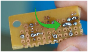
Although QFNs are packaged with many benefits for the consumers, they pose serious reliability and manufacturing concerns. Typically, defects such as voids, opens, shorts, and deficiencies are issues manufacturers grapple with when using this cutting-edge technology.
To produce QFNs that work optimally, proper inspection processes should be followed. However, inspection processes during production must be supported by accurate and reliable testing technologies that can identify even the minutest defects that can affect the performance of the devices.
QFN X Ray testing technique is the most appropriate and reliable one. By using x ray inspection methods, the Quality Control Department can identify soldering defects found in the QFN components, which may pose serious functional issues for the PCB.
How Does an X-Ray Machine Inspect QFN Components?
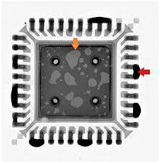
An X-ray inspection machine works by generating x-rays that illuminate the internal structure of the QFN component’s solder alloy. These x-rays are intense enough to penetrate the chip and create an image on the radiograph film. The resultant image is crucial because it gives a complete view of the QFN components solder structure defects.
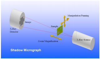
Being a non-destructive inspection method, you can be sure that the QFN component won’t be damaged in the inspection process. By design, the QFN x ray inspection machine provides real-time results enabling you to take quick remedial action before mass production of QFN components. Besides, x-ray inspection can offer a complete 3D image which gives a complete view of the component where even minute defects can be detected and corrected.
Other than detection, QFN X ray inspection can provide qualitative and quantitative analysis of the defects identified.
What Do I Need To Pay Attention to in the Process of QFN Testing?
While running the QFN testing process, you to pay attention to
Image Resolution
By using a high-resolution x-ray inspection machine, your results are clear and defects, which would otherwise be difficult to notice, become apparent.
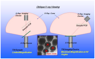
Viewing Angle
Generally, inspecting your sample at an oblique angle allows you to quickly find defects such as open joints, voids, cracks, and solder bridges.
Ability To Produce 3D Images
While 2D images are clear and good, 3D images are more detailed and are important in comprehensive and quality defect analyses.
What Defects Can the X-Ray Machine Detect in QFN Components?
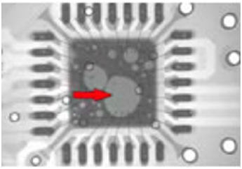
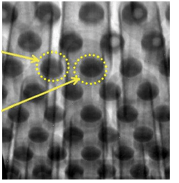
Voiding Defect
During the reflow process, the outgassing of entrapped flux in the sandwiched solder causes voids. Because they lack leads, QFNs have no standoffs that allow volatile escape or even stress absorption. Simply put, voids are cavities formed in the solder joint. Consequently, the board’s mechanical reliability and connection performance are affected.
How To Minimize Voiding
● Adding Vias to the Pad
Adding vias is one of the best methods of avoiding ground pad voids. By adding a via right from the design stage, you give room for the outgassing of the volatiles, which eventually reduces the formation of voids.
While this method is good, most contract manufacturers don’t have the luxury of applying it. This is because they have little influence on the board design, which is already designed and manufactured.
● Decreasing Aperture Sizes
Research has shown that you can minimize voids by reducing aperture size by about 30-50%.
● Stencil Thickness
Using a thinner stencil, say 4mil, as opposed to thicker ones, say 5mil, helps minimize voiding. It’s, however, important to say that this thickness shouldn’t be so much reduced since it can negatively impact the I/O pad solder connections.
● Pad and Placement Design
For successful QFN soldering, even and consistent placement pressure and depth are essential. You should apply tension on all sides of the component. To help maintain tension and allow easy outgassing, you can slightly move the pads outward by about 15-20%.
Solder Bridging Defect
Solder bridging occurs when too much solder is used to connect two more pads. And the name shouldn’t confuse you: a solder bridge isn’t easy to detect and requires an x-ray machine to detect.
Unfortunately, even a minute solder bridge can lead to disastrous results such as short-circuiting or component burns.
What Causes a Solder Bridge?
● Using a wrong stencil which puts too much solder on the SMT pads
● Applying an insufficient layer of solder resistance between the board’s pads
● Using big solder pads that aren’t consistent with the size of gaps between the pads
It’s a fact that having solder bridges on your QFN components is bad news. However, the good news is that there are various preventive mechanisms that you can apply.
How To Prevent Solder Bridges
● Leaving a Solder Mask Dam Between Pads
To prevent the occurrence of solder bridges, it’s good to leave a solder mask dam that isolates your pads by acting as a wall. The pad solder on one pad can spill over onto the other pad if you fail to leave the dam, and this can cause an unplanned solder bridge.
● Incorporating Mask Reliefs in the Board Design
By definition, a mask relief is an area on the board layout that doesn’t need the solder mask application. Typically, a mask relief appears as a thin outline around the surface mount pads, vias, and test points.
Non-Wetting or De-Wetting Defects
When molten solder fails to bond with the base metal, it creates a non-wetting defect. In this case, the PCB pads won’t securely stick together, affecting the board’s quality.
Non-wetting defect
On the other hand, De-wetting occurs when the molten solder initially coats the component terminals but then recedes after that. Consequently, it leaves behind thin solder areas on the base metal and thick, irregular lumps.
What Causes QFN Non-Wetting Defects?
● Using degraded flux
● Using the wrong type of flux
● Inadequate PCB Finish
● Poorly applying the board resin
● Using low soldering temperatures
● Using contaminated solder paste
Conclusion
Inspecting QFN components during or after production is an integral part of ensuring the quality of items and guaranteeing their functions. As the need for smaller yet powerful electronic items grows, QFN technology is almost indispensable.
However, effective testing of QFN components requires the most current inspection technology, which provides reliable results. This way, the company can produce PCBs that are beyond reproach hence promoting their brand and saving it from product recall costs.
Uni X-ray is a professional manufacturer of X-ray machines, they produces a wide range of X-ray machines to meet the needs of PCB inspection.
No comments:
Post a Comment