This article will discuss resistance temperature detector (RTD) circuit design for a functionally safe system and the Route 2S component certification process. Certifying a system is a long process as all components in the system must be reviewed for potential failure mechanisms and there are various methods to diagnose failures. Using parts that are already certified eases this workload along with the certification process.
Mary McCarthy , Applications Engineer, and Wasim Shaikh , Applications Engineer

Temperature is a key measurement in process control systems. It can be a direct measurement, measuring the temperature of a chemical reaction. It may also be a compensation measurement—for example, temperature compensation of a pressure transducer. For any system design, it is critical that this measurement is accurate, reliable, and robust. For some end designs, it is critical that system failures are detected and if the system fails, it transitions to a safe state. Functionally safe designs are used in these environments. The level of certification indicates the level of diagnostic coverage included in the design.
What Is Functional Safety
In a functionally safe design, any failures need to be detected by the system. Think of an oil refinery where a tank is being filled. If a failure of the level sensor occurs, it is important that this failure is detected so that the valve to the tank can be actively shut off. This will prevent a tank overflow and avoid a potentially hazardous explosion. Alternatively, redundancy can be used. This is where two level sensors can be used in the design so that the system can continue functioning with the second level sensor when the first level sensor fails. When a design is certified, it is given a SIL rating. This rating indicates the diagnostic coverage provided by the design.
The higher the SIL rating, the more robust the solution. A SIL 2 rating indicates that over 90% of failures within the system can be diagnosed. To certify a design, the system designer must provide evidence to the certification house on the potential failures, whether these are safe failures or hazardous failures and how the failures can be diagnosed. Data such as FIT are needed along with failure modes effects and diagnostic analyses (FMEDAs) on the different components in the system.
Designing a Temperature System
In this article, we will focus on RTDs. However, there are many different types of temperature sensors—RTDs, thermistors, and thermocouples. The sensor to use in a design depends on the accuracy required and the temperature range being measured. Each sensor type has its own requirements:
• Biasing of thermocouples
• Excitation currents to excite an RTD
• An absolute reference for thermocouples and thermistors
So, along with the ADC, other building blocks are needed to excite the sensor and condition the sensor on the front end. For functional safety, all these blocks must be reliable and robust. In addition, any failures of the different blocks must be detectable. Traditionally, a system designer used duplication so two signal chains would be used with each signal chain checking the other to ensure:
• The sensor is connected
• There are no opens or shorts
• The reference is at the correct level
• The PGA is still functioning
Documentation is needed for the certification process to prove the design is robust. This is a time-consuming process and sometimes some of the information is difficult to obtain from the IC manufacturers.
However, the AD7124-4/AD7124-8 integrated analog front ends now include all the building blocks needed for an RTD design. In addition, embedded diagnostics eliminate the need for signal chain duplication for diagnostic purposes. Along with the silicon enhancements, Analog Devices provides documentation that includes all the information required by the certification houses (FIT pin FMEDA, die FMEDA). This eases the certification process for functional safety.
IEC 61508 is the specification for functionally safe designs. This specification documents the design flow needed to develop a SIL certified part. Documentation needs to be generated for each step, from concept, definition, design, layout, fabrication, assembly, and test. This is known as Route 1S. Another option is to use the Route 2S flow. This is a proven in use route so, when large volumes of the product have been designed into end customer’s systems and used in the field for 1000s of hours, a product can still be certified by providing evidence to the certification house of:
• Volumes used in the field
• Analysis of any returns from the field and detail that the returns were not due to failures within the component itself
• Safety data sheet giving detail on the diagnostics and the coverage they provide
• Pin and die FMEDA
3-Wire RTD Design
RTDs
RTDs are useful for measuring temperatures in the range of –200°C to +850°C and have a near linear response over this temperature range. Typical elements used for RTDs are nickel, copper, and platinum, with 100 Ω and 1000 Ω platinum RTDs being the most common. An RTD is made up of either two, three, or four wires, with 3-wire and 4-wire being the most used. These are passive sensors that require an excitation current to produce an output voltage. The output voltage levels of such RTDs vary from 10s of millivolts to 100s of millivolts depending on the RTD chosen.
RTD Design
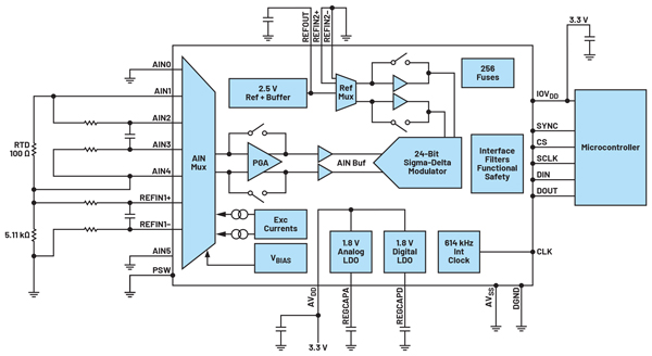
Figure 1 shows a 3-wire RTD system. The AD7124-4/AD7124-8 are an integrated solution for RTD measurement that includes all the building blocks needed for the system. To fully optimize this system, two identically matched current sources are needed. These two current sources are used to cancel the lead resistance errors produced by RL1. One excitation current flows through both the precision reference resistor, RREF, and the RTD. The second current flows through lead-resistance RL2 and develops a voltage that cancels the voltage drop across RL1. The voltage generated across the precision reference resistor is used as the reference voltage REFIN1(±) to the ADC. Since one excitation current is used to generate both the reference voltage and the voltage across the RTD, the current source accuracy, mismatch, and mismatch drift have a minimal effect on the overall ADC transfer function. The AD7124-4/AD7124-8 offer a choice of excitation current values that allows the user to tune the system so that most of the ADC input range is used, resulting in increased performance.
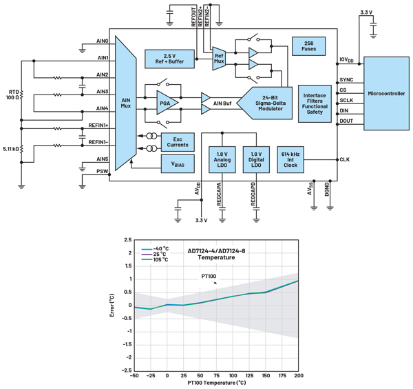
The low level output voltage from the RTD needs to be amplified so that most of the ADC’s input range is used. The AD7124-4/AD7124-8’s PGA is programmable from a gain of 1 to 128, allowing the customer to trade off excitation current value vs. gain and performance. Filtering is required between the sensor and the ADC for antialiasing and EMC purposes. Reference buffers allow unlimited values for the R and C components of the filter; that is, these components do not impact the accuracy of the measurement.
Calibration is also required in the system to eliminate gain and offset errors. Figure 1 shows the temperature error measured for this 3-wire Class B RTD following an internal zero-scale and full-scale calibration, the overall error being much less than ±1°C.
ADC Requirements
For temperature systems, the measurements are mainly low speed (up to 100 samples per seconds typically). Therefore, a low bandwidth ADC is required.
However, the ADC must have high resolution. Sigma-delta ADCs are suitable for these applications since low bandwidth, high resolution ADCs can be developed using the sigma-delta architecture.
With sigma-delta converters, the analog input is continuously sampled, the sampling frequency being considerably higher than the band of interest. They also use noise shaping that pushes noise out of the band of interest into a region not being used by the conversion process, further reducing the noise in the band of interest. The digital filter attenuates any signal outside the band of interest.
The digital filter does have images at the sampling frequency and multiples of the sampling frequency. Hence, some external antialiasing filters are required.
However, due to the oversampling, a simple first-order RC filter is sufficient for most applications. The sigma-delta architecture allows 24-bit ADCs with a p-p resolution of up to 21.7 bits to be developed (21.7 stable or flicker free bits).
Other benefits of the sigma-delta architecture are:
• Wide common-mode range for the analog inputs
• Wide common-mode range for the reference inputs
• Ability to support ratiometric configurations
Filtering (50 Hz/60 Hz Rejection)
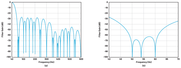
Along with rejecting the noise as discussed previously, the digital filter is also useful to provide 50 Hz/60 Hz rejection. Interference occurs at 50 Hz or 60 Hz when systems are operated from the mains power supply. There are mains generated frequencies at 50 Hz and its multiples in Europe and 60 Hz and its multiples in the U.S. The low bandwidth ADCs mainly use sinc filters, which can be programmed to set notches at 50 Hz and/or 60 Hz along with multiples of 50 Hz and 60 Hz, thereby providing rejection at 50 Hz/60 Hz and their multiples.
There is an increasing requirement to provide 50 Hz/60 Hz rejection using filtering methods that have low settling time. In a multichannel system, the ADC sequences through all enabled channels, generating a conversion on each.
When a channel is selected, it requires the filter settling time to generate a valid conversion. The number of channels converted in a given period of time is increased if the settling time is reduced. The AD7124-4/AD7124-8 include postfilters or FIR filters, which provide simultaneous 50 Hz/60 Hz rejection at lower settling times compared to a sinc3 or sinc4 filter. Figure 3 shows one digital filter option: this postfilter has a settling time of 41.53 ms and provides simultaneous 50 Hz/60 Hz rejection of 62 dB.
Diagnostics
For a functionally safe design, diagnostics are required for all the functions making up the RTD system. As the AD7124-4/AD7124-8 have multiple embedded diagnostics, this simplifies the design complexity and design time. It also removes the need to duplicate the signal chain for diagnostic coverage.
Typical diagnostic requirements are:
• Power supply/reference voltage/analog input monitoring
• Open wire detection
• Conversion/calibration checks
• Signal chain functionality check
• Read/write monitoring
• Register content monitoring
Let’s look at the embedded diagnostics in more detail.
SPI Diagnostics
CRC is available on the AD7124-4/AD7124-8. When enabled, all read and write operations include a CRC calculation. The checksum, which is 8-bit wide, is generated using the polynomial
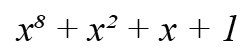
So, for every write to the AD7124-4/AD7124-8, the processor generates a CRC value that is appended to the information being sent to the ADC. The ADC generates its own CRC value from the information received and compares it against the CRC value received from the processor. If both values agree, this ensures that the information is intact and will be written to the relevant onchip register. If the CRC values do not match, this indicates that bit corruption have occurred in the transmission. In this case, the AD7124-4/AD7124-8 set an error flag that indicates that data corruption has occurred. They also self protect by not writing the corrupt information into a register. Similarly, when information is being read from the AD7124-4/AD7124-8, they will generate a CRC value to accompany the information. The processor will process this CRC value to determine if the transmission is valid or corrupted.
The AD7124-4/AD7124-8 data sheets list the registers that can be accessed by customers (user registers). The AD7124-4/AD7124-8 check the addresses of registers being accessed. If a user attempts to read from or write to a register not documented in the data sheet, an error flag is set, indicating that the processor is attempting to access a nonuser register. Again, any information that accompanies this register access is not applied to the registers.
The AD7124-4/AD7124-8 also have an SCLK counter. All read and write operations are a multiple of eight. When CS is used to frame read and write operations, the SCLK counter counts the number of SCLK pulses used in each read/write operation while CS is low. When CS is taken high, the number of SCLKs used in the communication should be a multiple of eight.
If glitching occurred on the SCLK, this would lead to excess SCLK pulses. If this occurs, the AD7124-4/AD7124-8 again set an error flag and they abandon any information entered.
The status register indicates the channel being converted. When the data register is read, the status bits can be appended to the conversion result. This adds another layer of robustness to the processor/ADC communications.
So, all the diagnostics mentioned ensure that the communications between the ADC and the processor are robust. They ensure that only valid information is accepted by the AD7124-4/AD7124-8. When CS is used to frame read and write operations, the serial interface is reset each time that CS is taken high. This ensures that all communication begins from a defined or known state.
Memory Checks
Each time the on-chip registers are altered (changing the gain for example), a CRC is performed on the registers and the resulting CRC value is temporarily stored internally. Periodically, the AD7124-4/AD7124-8 internally perform additional CRC checks on the registers. The resulting CRC values are compared against the stored value. If the values differ due to a bit flip, a flag is set. This indicates to the processor that the register settings have been corrupted. The processor can then reset the ADC and reload the registers.
The on-chip ROM holds the default register values. On power-up or following a reset, the ROM contents are applied to the user registers. In the final production test, the CRC for the ROM contents is calculated and the resulting CRC value is stored in ROM. At power-up or reset, a CRC is again performed on the ROM contents and the resulting CRC value is compared against the saved value. If the values differ, this indicates that the default register settings will not be as expected. Power cycling or a reset is needed.
Signal Chain Checks
Numerous signal chain checks are included. The power supply rails (AVDD, AVSS, and IOVDD) can be applied to the ADC input, allowing the power supply rails to be monitored. The AD7124-4/AD7124-8 include an analog and a digital low dropout (LDO) regulator internally. These can also be applied to the ADC and monitored.
The AD7124-4/AD7124-8 include x-multiplexing. In addition, AVSS can internally be used as AIN-. This allows the absolute voltage on the analog input pins to be checked. So, a customer can probe the pins on which the excitation current is output and probe the AIN+ and AIN– pins. This will check for connectivity and ensure the voltages on the various pins are at the correct level.
To check the reference voltage, the reference detect function will indicate that the reference voltage is too low. The customer can also select the internal reference as an analog input so this could be used to monitor the voltage generated across the external reference resistor. This assumes that the voltage across the reference resistor is slightly higher than 2.5 V (magnitude of the internal reference).
The AD7124-4/AD7124-8 also include an internal 20 mV. This is useful to check the gain stage. For example, with the 20 mV as the analog input, the gain can be changed from 1 to 2, 4, … 128. The conversion result will scale by a factor of 2 each time the gain is increased, which confirms that the gain stage is functioning correctly.
X-multiplexing is also useful when checking for stuck bits. It allows the AIN+ and AIN– pins to be swapped. The conversion result is then inverted. So, using the 20 mV along with the x-multiplexing allows the user to check for stuck bits.
Selecting the same analog input pin for AIN+ and AIN– and biasing this internal short allow a check on the ADC noise to ensure it is working within specification. The embedded reference (+2.5 V) can be selected internally as an input to the ADC so, again, applying +VREF and –VREF is useful to confirm the signal chain is functioning correctly.
Burnout currents that are programmable are useful to check for sensor connectivity. A PT100 has a resistance of 18 Ω typically at –200°C and 390.4 Ω at +850°C. With the burnout currents enabled, a conversion can be performed.
If the RTD is shorted, a conversion result close to 0 will be obtained. An open wire between AIN+ and AIN– will result in a conversion close to 0xFFFFFF. With the RTD correctly connected, a code close to 0 or all 1s should never be obtained.
Finally, the AD7124-4/AD7124-8 have overvoltage and undervoltage detection. The absolute voltage on the AIN+ and AIN– pins being converted is continuously monitored via comparators. Flags are set when the voltage on AIN+ or AIN– goes outside the power supply rails (AVDD and AVSS).
This high level of integration reduces the bill of materials (BOM) needed to perform the measurement and to provide the diagnostics coverage. Design time and design complexity are reduced.
Conversion/Calibration
Conversions on the AD7124-4/AD7124-8 are also monitored. If (AIN+ – AIN–)/gain is greater than +full-scale or less than –full-scale, a flag is set. The conversion from the ADC goes to all 1s (analog input too high) or all 0s (analog input too low) so the customer knows that a fault has occurred.
The bit stream from the modulator is monitored to ensure that the modulator does not saturate. If saturation occurs (20 consecutive 1s or 20 0s output from the modulator), a flag is set.
The AD7124-4/AD7124-8 include internal offset and again calibration and system offset and gain calibration. If the calibration fails, this is flagged to the user.
Note that the offset and gain registers are not updated if a calibration fails.
Power Supplies
Along with the power supply checks discussed earlier, the AD7124-4/AD7124-8 include comparators that continuously monitor the internal LDO regulators.
So, if the voltages from these LDO regulators fall below the trip point, the errors are reported immediately.
These LDO regulators require an external capacitor. The presence of this capacitor can also be checked.
MCLK Counter
The filter profile and output data rate are directly related to the MCLK. The output data rates listed in the data sheet are correct when the master clock is 614.4 kHz. If the master clock changes frequency, the output data rate and the filter notches will also change. If the filter notches are used to reject 50 Hz or 60 Hz, for example, a varying clock reduces the attenuation obtained. Therefore, knowing the clock frequency is valuable to ensure that optimum rejection is obtained. The AD7124-4/AD7124-8 include an MCLK counter register. This register is incremented by 1 every 131 MCLK cycles. To measure the MCLK frequency, a timer in the processor is needed. The register can be read at time 0 and then read after the timer times out. With this information, the frequency of the master clock can be determined.
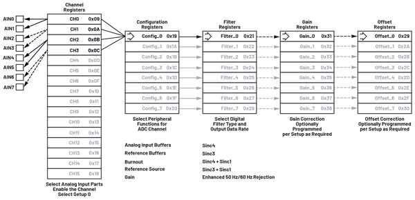
Per Channel Configuration
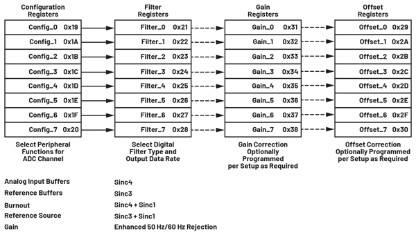
The AD7124-4/AD7124-8 allow per channel configuration; that is, they support eight different setups, a setup consisting of the reference source, gain setting, output data rate, and a filter type. When the user configures a channel, one of the eight setups is assigned to the channel. Note that the channel can be an analog input or a diagnostic such as measuring the power supply (AVDD-AVSS).
So, a customer could design a sequence to be made up of analog inputs and diagnostics. The per channel configuration allows the diagnostic to be operated at a different output data rate to the analog input conversion. As diagnostics do not require the same accuracy as the main measurement, the customer can interleave diagnostics with measurements and run the diagnostics at a higher output data rate. So, these embedded features reduce the workload of the processor.
Other Functionality
The AD7124-4/AD7124-8 include a temperature sensor, which also can be used to monitor the die temperature. Both parts have an ESD rating of 4 kV, leading to a robust solution. Both parts are housed in a 5 × 5 mm LFCSP package, an option that is suitable for intrinsic safe designs.
The FMEDA of a typical temperature application using these devices has shown a safe failure fraction (SFF) greater than 90% according to IEC 61508. Two traditional ADCs are normally required to provide this level of coverage.
Additional Benefits of Built-In Diagnostics
Apart from BOM and cost savings, the diagnostics also lead to savings in terms of avoiding design complexity, reducing resource usage, and achieving faster time to market for customers. Let’s understand this with the help of the following example:
The AD7124-4/AD7124-8 feature an MCLK counter, which is used to measure the main clock frequency and catch any kind of inconsistencies in the master clock provided. The master clock counter is an 8-bit register, which is incremented every 131 MCLK cycles. This register is read by the SPI master to determine the frequency of the internal/external 614.4 kHz clock.
What if I had to implement the MCLK frequency check external to the AD7124-4/AD7124-8? It will need these hardware resources:
• Microcontroller with a peripheral, like a counter and an external interrupt controller
• Schmitt trigger circuit
Also, note that there will be memory needed to store and run the code that will include interrupt service routines. Overall, the scheme would be as shown in Figure 5.
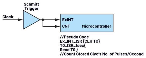
Additionally, we have to make sure that the code is checked and is in line with coding guidelines and restrictions. So overall, there would be significant overhead to implement a separate section of diagnostics; hence, the built-in diagnostics bring additional benefits:
• Space and BOM savings
• Improved system reliability; fewer components = better reliability
• Faster time to market
• Software development—develop and run routines for diagnostics
• Hardware testing
• System testing
• Microcontroller memory savings
• Don’t need code for running diagnostics
• Coding guidelines ask for a lot of double memory code checking
• Ready to use safety documentation saves system assessment time
Aiding Functionally Safe Design
The AD7124-4/AD7124-8 are not SIL rated, meaning that they are not designed and developed using development guidelines as per IEC 61508 standard.
However, by understanding the end application and usage of various diagnostics, one can assess the AD7124-4/AD7124-8 for usage in a SIL rated design.
Functional Safety Terminologies
Let’s review some of the concepts important to the certification journey:
• Failures: systematic and random
• Diagnostic coverage
• Hardware fault tolerance
• SIL levels
Failures: Systematic and Random
Systematic failures are deterministic (nonrandom) failures from a certain cause, which can be eliminated by a modification of the design or of the manufacturing process, operational procedures, documentation, or other relevant factors. For example, a noisy interrupt to the system happens due to a lack of filtering on the external interrupt pin.
On the other hand, random failures are due to physical causes, which apply to hardware components within a system. This type of fault is caused by effects such as corrosion, thermal stressing as well as wear-out and it is not possible to catch such failures by systematic processes.
To deal with random failures, we can use methods like reliability, diagnostics, and redundancy.
In reliability, we ensure usage of reliable components, while with diagnostics we make sure that these failures can be detected and corrected. Another way to ensure reliability is to add redundancy to lower the probability of failure but then we increase the system cost and space.
There are four types of random failures, which are safe detected, safe undetected, dangerous detected, and dangerous undetected.
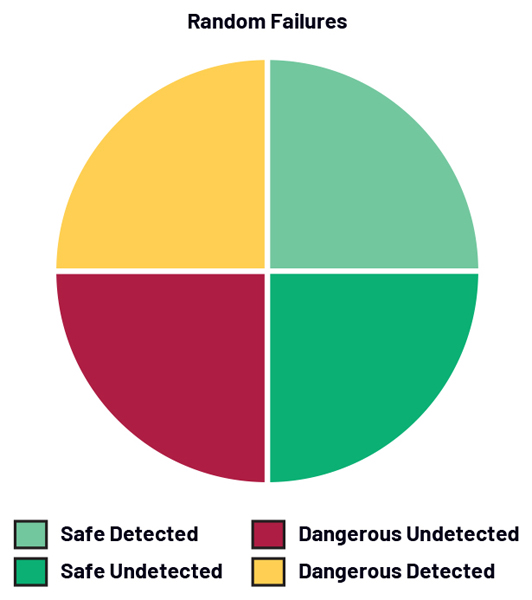
For example, consider a system whose safety function is to open up a power switch for the machine when the temperature read is high. Any random failure that does not impact the safety function, that is, opening up the power switch, is termed a safe detected or a safe undetected failure. The other malfunctions impacting the safety function are dangerous failures. The most important one for us is the dangerous undetected failure. This failure type is the one not covered by diagnostics, so our goal is to increase the diagnostics to keep the dangerous undetected failures minimal.
Diagnostic Coverage
Random failures can be detected by having various built-in detection mechanisms in the form of software or hardware. For example, a failure in a MOSFET switch can be detected by reading back the output or a random memory bit flip can be detected by running CRC memory checks on regular intervals.
Diagnostic coverage is the ability of the system to detect dangerous failures, mathematically defined as the ratio of dangerous detected failures to dangerous failures.
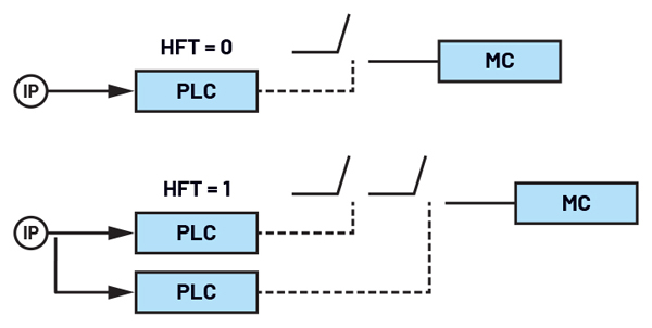
Hardware Fault Tolerance
Consider a programmable logic controller (PLC) system, such as the one shown in Figure 7, whose safety function is to open the switch in order to stop the machine if the input goes beyond a particular value. In the HFT = 0 figure, if there is a single random failure (X) then the system will malfunction and the machine will not stop.
Now, if we have a redundant path as shown in the HFT = 1 figure, then a single random failure will no longer cause the failure and we will be able to stop the machine.
So, by adding a redundant path, a single failure can be tolerated; this system is called HFT 1 system, which says that one failure cannot cause the system to fail.
HFT 0 means one failure can cause the system to fail. Hardware fault tolerance is the ability of a component or subsystem to perform a safety function in the presence of one or more dangerous faults.
HFT can be calculated from architectures like 1oo1, 1oo2, 2oo3, etc. If the architecture is expressed as MooN, then the HFT is calculated as N – M. In other words, a 2oo4 architecture has an HFT of 2. This means it can tolerate two failures and it still works, and thus it is an architecture with redundancy.
SIL Level Coverage
Table 1 plots SFF (which is the amount of diagnostic coverage) and hardware fault tolerance (meaning the redundancy).
The rows show the amount of diagnostic coverage, whereas the columns show the hardware fault tolerance. HFT of 0 means that if there is one fault in the system, the safety function will be lost (see Table 1).
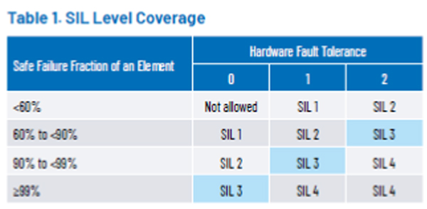
If we add redundancy achieving HFT 1 as shown in Figure 7, the system can tolerate one failure without the system going down. So, customers who achieve SIL 3 with redundancy today could achieve a SIL 3 rating without redundancy if they use a part with higher diagnostic coverage.
So, with a higher level of diagnostics we reduce the amount of system redundancy needed, or we improve the SIL level of the solution with the same level of redundancy (move down on Table 1).
Now, let’s recall the diagnostics in the AD7124-4/AD7124-8, which support various built-in mechanisms like power supply/reference voltage/AIN monitoring, open wire detection, conversion/calibration checks, signal chain functionality check, read/write monitoring, register content monitoring, etc. that boost the diagnostic coverage of the AD7124-4/AD7124-8 system. In the absence of these diagnostics, two ADCs would be required to achieve the same desired level.
Hence, one AD7124-4 or AD7124-8 provides the same level of coverage and its diagnostic coverage and features enable design for a functionally safe system. This results in 50% savings in BOM and printed circuit board space.
Documentation to Support SIL Rated Designs
The documentation needed for aiding end system SIL certification are:
• Safety data sheet (the safety manual is for a SIL rated part)
• Pin FMEDA (failure modes, effects, and analysis) and die FMEDA (failure modes, effects, and diagnostic analysis)
• Annex F checklist
These documents are comprised of inputs, primarily from four sources of data, as shown in Figure 8. These data are diagnostic data, design data, FIT rates, and data from fault insertion tests.
• Diagnostic data from the data sheet capture all the diagnostic features available in the part.
• Design data refers to internal data—for example, the die area and impact of each and every internal block of the part.
• FIT, or failure in time, rates for various components are available from the data book. A popular example is the Siemens Databook SN 29500.
• Fault insertion tests are done for blocks, which cannot be analyzed using design and diagnostic data. These tests are planned based on the application required, and the outcome of fault insertion tests is used to strengthen the FMEDA and FMEA documents.
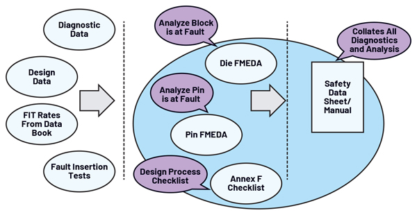
Die FMEDA
The AD7124-4/AD7124-8 FMEDA analyzes the main blocks in the application schematic, identifies failure modes and effects, and checks the diagnosis and analyses for a particular safety function. Let’s look at Figure 9 to understand the mechanism.
For an RTD type system, the safety function is to measure temperature with an accuracy of ±x degree; the application schematic is shown in Figure 9.
We define a dangerous fault as a fault that can le ad to an error in the ADC output or SPI communication, and if the error in the output is significant, it can cause a dangerous failure.
Safe state is defined as:
• Data on the output represent the input as per the safety function
• An error status bit is set
• ADC output conversion result is all zeroes or all ones
• No SPI communication
The AD7124-4/AD7124-8 are identified as a Type B system according to IEC 61508. To explain the FMEDA, let’s take the example of the clock module and analyze its failure modes.
Table 2 shows what happens when the clock block faces the failure modes described in the first column, its effect on output, the amount of diagnostic coverage, and lastly the analysis.
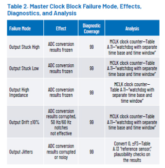
Similarly, we then analyze the remaining blocks in the AD7124-4/AD7124-8.
Note that there may be some failures that may not impact the safety function; for example, the failure on the AIN0 pin will not cause problems for temperature measurement and, hence, can be excluded from the safety calculations. The outcome of the FMEDA will be failure rates of safe failures, dangerous detected failures, and dangerous undetected failures, which are used to calculate the SFF.
Pin FMEDA
The pin FMEDA analyzes various types of failures on the pins of the AD7124-4/AD7124-8 and their outcome for this RTD application. Step by step, we take every individual pin and analyze the outcome in case the pin opens up or shorts to supply/ground or shorts to adjacent pins.
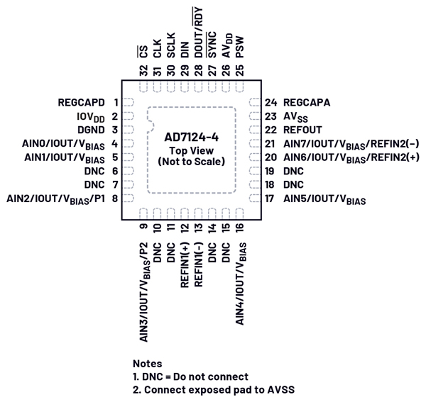
For example, let’s take Pin 29 (DIN) from Figure 10, refer to the application schematic shown in Figure 9, and check the outcome for different failures. Table 3 shows the failure mode, effects, and detection.
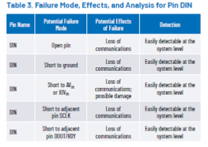
Note that the analysis is with respect to the application schematic shown in Figure 9, so the analysis of an unused pin will not impact anything.
Annex F Checklist
This is a design measures checklist for ASICs avoidance of systematic failures.
A completed Annex F checklist from IEC 61508-2:2010 is needed for compliance.
Safety Manual or Data Sheet
An entire set of information finally flows into the safety manual or data sheet, which provides the necessary requirements to enable the integration of the AD7124-4/AD7124-8.
When showing compliance with the IEC 61508 functional safety standards, the safety data sheet collates all the diagnostics and analyses that flow in from various documents. It will have all the information such as:
• Product overview
• Application information
• Safety concept
• Lifetime predictions
• FIT
• FMEDA calculations—SFF and DC
• Hardware safety mechanisms
• Diagnostics description
• EMC robustness
• Operation in redundant configurations
• Annexures and document list
Route 2S, Also Known as Proven in Use
We have discussed the first method for assessment. Now, let us discuss the alternate method known as proven in use or Route 2S. This method is applicable for a released part and is based on an analysis of customer returns and the number of devices shipped.
This allows SIL certification as if the part was fully developed as per the IEC 61508 standard.
Route 2S or a proven in use claim may be available to module/system designers if they have successfully used an IC in the past and know the failure rate from the field.
Note that, in Route 2S, we need the entire data of field returns, which makes this claim much harder for integrated circuit designers or manufacturers as they generally do not have enough knowledge of the final application or what percentage of the failing units from the field are returned to them for analysis.
Conclusion
The ADC and system requirements for an RTD measurement system are quite stringent. The analog signals generated by these sensors are small. These signals need to be amplified by a gain stage whose noise is low so that the amplifier’s noise does not swamp the signal from the sensor. Following the amplifier, a high resolution ADC is required so that the low level signal from the sensor can be converted into digital information. Along with the ADC and gain stage, a temperature system requires other components such as excitation currents. Again, these must be low drift, low noise components so that the system accuracy is not degraded. Initial inaccuracies such as offset can be calibrated out of the system but the drift of the components with temperature must be low to avoid error introduction. So, integrating the excitation blocks and measurement blocks simplifies the customer design. When designing for functional safety, there is the additional need for diagnostics. By integrating diagnostics along with the excitation and measurements blocks, the overall system design is eased, reducing the BOM, design time, and time to market.
Documentation such as FMEDAs contains all the information required by customers to certify the component in the end design. However, certifying the components themselves eases the conversation with the certification house further. The Route 2S process allows products to be certified postrelease so this is a useful route as there are many devices currently released, which suit functionally safe designs.
About the Authors
Mary McCarthy is an applications engineer at Analog Devices. She joined ADI in 1991 and works in the Linear and Precision Technology Applications Group in Cork, Ireland, focusing on precision sigma-delta converters. Mary graduated with a bachelor’s degree in electronic and electrical engineering from University College Cork in 1991.
Wasim Shaikh joined Analog Devices in 2015 as an applications engineer in the Precision Converters Department located in Bangalore, India. Wasim is a certified functional safety engineer and received his bachelor’s degree from Pune University in 2003.
No comments:
Post a Comment